About

Über uns

At Elastic-Simulations we develop specialized and automated simulation processes ready for massive parallelization in the cloud to serve our customers the most advanced and highly cost-efficient simulation capabilities for special simulation tasks. At Elastic-Simulations we are convinced that automation and cloud-computing is the future of simulation and virtual prototyping. Enthusiasm for automation and cloud computing is therefore ingrained in our DNA.

Bei Elastic-Simulations entwickeln wir spezialisierte und automatisierte Simulationsprozesse, welche für eine massive Parallelisierung in der Cloud bereit sind, um unseren Kunden die fortschrittlichsten und höchst kosteneffizienten Simulationsmöglichkeiten für spezialisierte Simulationsaufgaben bereitzustellen. Wir bei Elastic-Simulations sind davon überzeugt, dass Automatisierung und Cloud-Computing die Zukunft der Simulation und des virtuellen Prototypings sind. Enthusiasmus für Automatisierung und Cloud-Computing sind daher tief in unserer DNA verwurzelt.


Icon showing software automation

Automation

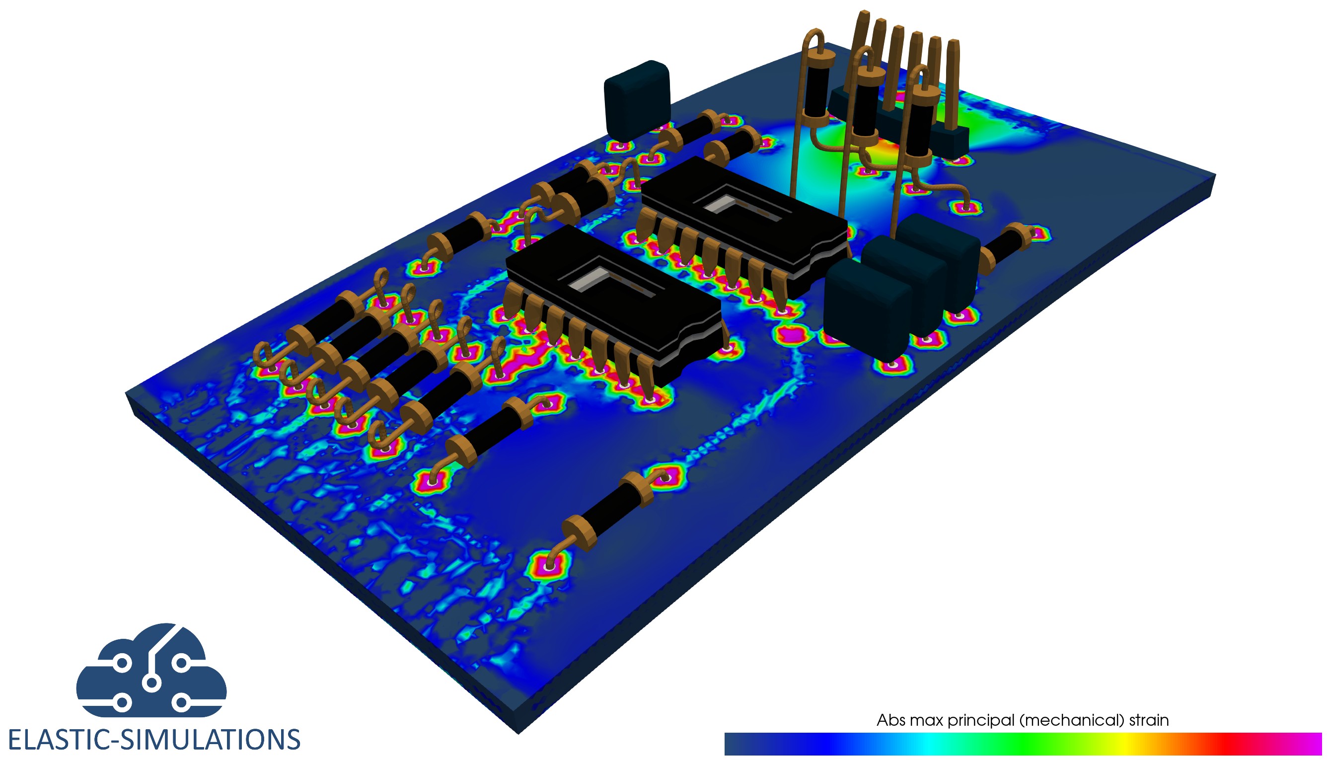
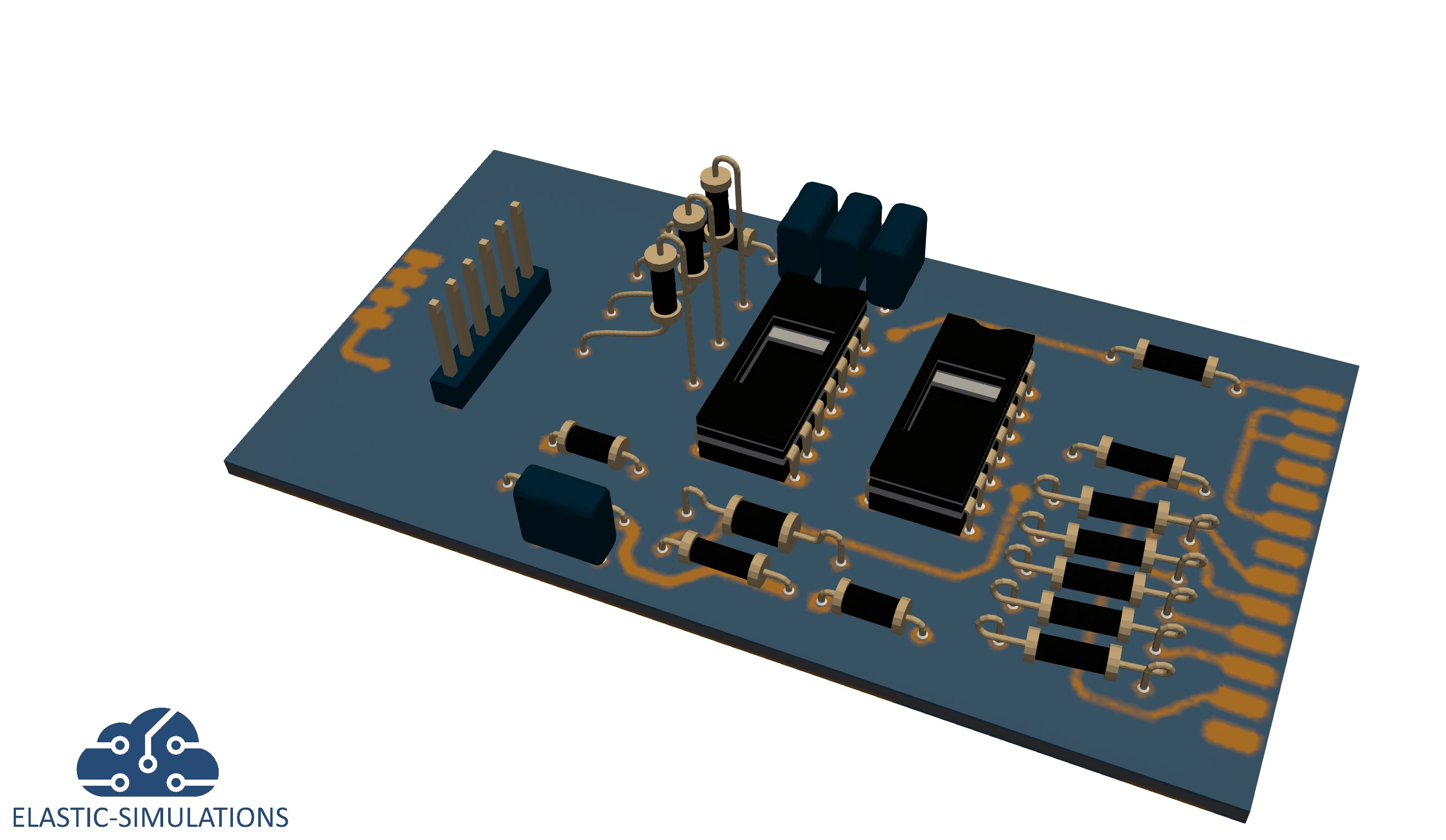
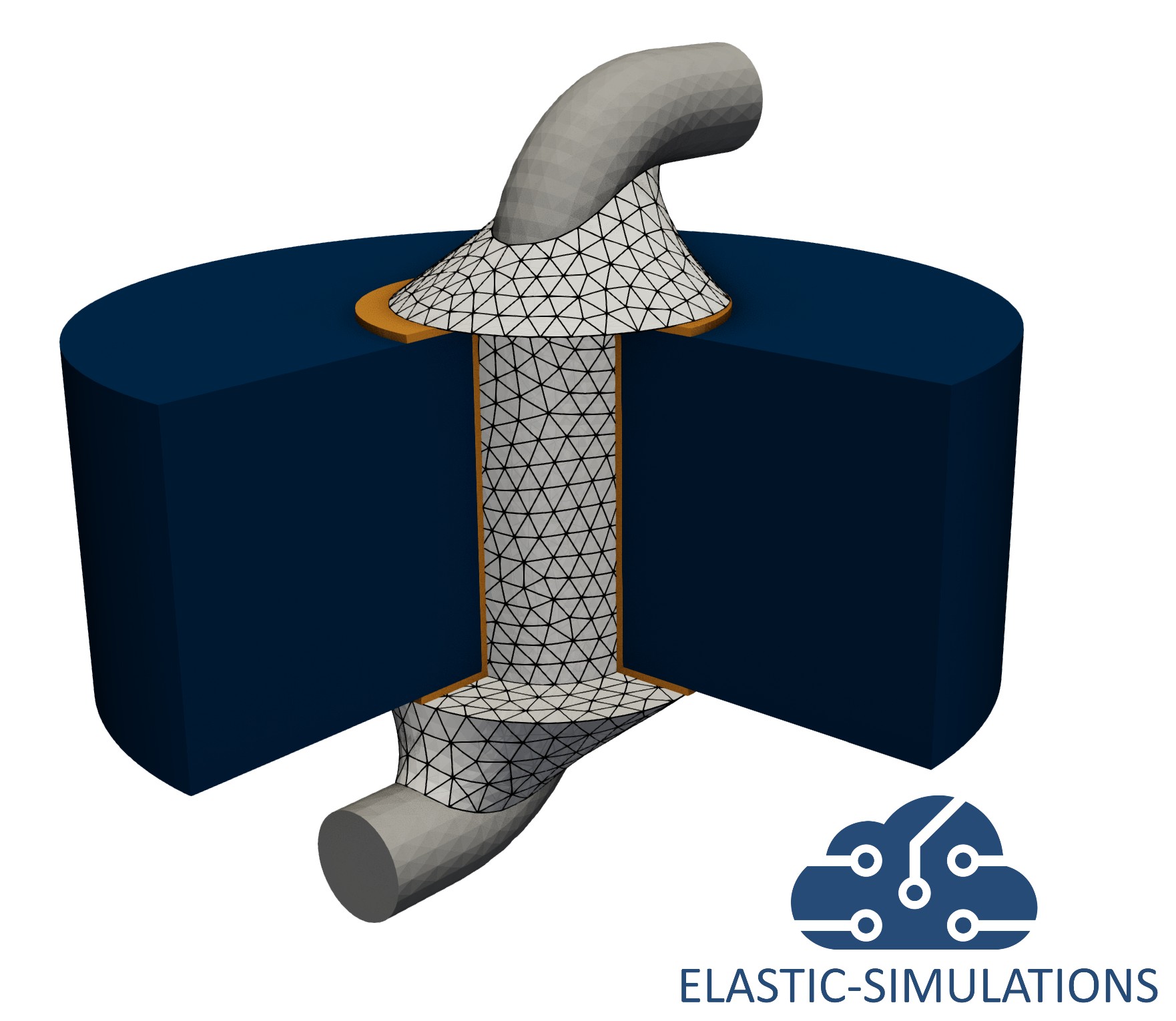
We automate the processing of complex modelling and simulation tasks. For the analysis of electronic components we automated the modelling of printed circuit boards, surface mounted devices, solder joints, vias, traces and more to meet the modelling detail requirements of our customers' simulation tasks.

Wir automatisieren die Bearbeitung komplexer Modellierungs- und Simulationsaufgaben. Für die Analyse von Elektronikkomponenten haben wir die Modellierung von Leiterplatten, Surface-Mounted Devices, Lötstellen, Vias, Leiterbahnen und mehr automatisiert, um die Detailanforderungen in der Modellierung der Simulationsaufgaben unserer Kunden zu erfüllen.

Icon showing computer simulations

Simulation

We develop specialized simulation processes for the analysis of electronic components. Based on our pre- and post-processing automation routines, printed circuit board assemblies can be simulated with an outstanding modeling quality, whereby even small copper tracks, vias or solder joints can be modeled and analysed.

Wir entwickeln spezialisierte Simulationsverfahren zur Analyse von Elektronikkomponenten. Basierend auf unseren Pre- und Post-Processing-Automatisierungsroutinen können bestückte Leiterplatten mit hervorragender Modellierungsqualität simuliert werden, wobei selbst kleine Kupferbahnen, Vias oder Lötstellen modelliert und analysiert werden können.

Icon showing parallelization on cloud infrastructure

Cloud-Computing

Our automation and simulation processes are ready for massive parallelization on cloud infrastructure. For the analysis of printed circuit boards the sub-structuring, sub-modelling and multi-scale modelling can be heavily parallelized to deliver simulation results as fast as possible.

Unsere Automatisierungs- und Simulationsprozesse sind bereit für eine massive Parallelisierung auf Cloud-Infrastruktur. Für die Analyse von bestückten Leiterplatten können Substrukturierung, Submodellierung und Multiskalenmodellierung stark parallelisiert werden, um Simulationsergebnisse so schnell wie möglich zur Verfügung zu stellen.

Services

Leistungen

Electronic components including printed circuit board assemblies (PCBAs) are subjected to various loads caused by handling, assembling, and operation conditions. The loads can be of static, dynamic, or thermo-mechanic form, which all result basically in bending of the PCBA and in applying stress to surface mounted devices, solder joints, vias, and traces. Thus, PCBAs have to qualified according to standardized tests like:

Elektronische Komponenten, einschließlich bestückter Leiterplatten (engl. printed circuit board assemblies, PCBAs), werden verschiedenen Belastungen ausgesetzt, welche durch Handhabung, Montage und Betriebsbedingungen verursacht werden. Die Belastungen können statischer, dynamischer oder thermo-mechanischer Form sein, welche alle im Wesentlichen zum Biegen der PCBA und zum Aufbringen von Spannungen auf oberflächenmontierte Bauteile (engl. surface mounted devices, SMDs), Lötstellen, Vias und Kupferbahnen führen. Daher müssen PCBAs zur Qualifizierung standardisierten Tests unterzogen werden wie z.B.:

At Elastic-Simulations we developed specialized and automated simulation processes for the static, dynamic, and thermo-mechanic analysis of PCBAs which can be used to reproduce these loads virtually. The simulation processes were developed with cloud infrastructure in mind; thus, the simulation complexity can be scaled based on the technical requirements and cost requirements of our customers. At Elastic-Simulations we believe that modelling of geometric details is key to retrieve accurate simulation results. Thus, our processes are based on detailed finite element models of solder joints, vias, and traces. Based on the cost requirements of our customers these detailed models can be used directly in the simulations or can be simplified to sub-structures or sub-models.

Bei Elastic-Simulations haben wir spezialisierte und automatisierte Simulationsprozesse für die statische, dynamische und thermomechanische Analyse von PCBAs entwickelt, mit welchen diese Belastungen virtuell reproduziert werden können. Die Simulationsprozesse wurden im Hinblick auf Cloud-Infrastruktur entwickelt; somit kann die Simulationskomplexität basierend auf den technischen Anforderungen und Kostenanforderungen unserer Kunden skaliert werden. Bei Elastic-Simulations sind wir davon überzeugt, dass die Modellierung von geometrischen Details der Schlüssel für genaue Simulationsergebnisse ist. Daher basieren unsere Prozesse auf detaillierten Finite-Elemente-Modellen von Lötstellen, Vias und Leiterbahnen. Basierend auf den Kostenanforderungen unserer Kunden können diese detaillierten Modelle direkt in den Simulationen verwendet oder zu Substrukturen oder Submodellen vereinfacht werden.


Simulation process for the static analysis of PCBAs

Simulationsprozess zur statischen Analyse von PCBAs

Printed circuit board assemblies (PCBAs) are subjected to various loads during handling and assembling. These loads can result in bending of a printed circuit board (PCB) and in pulling forces applied on a PCB. Especially the bending of PCBAs can cause failures of solder joints and surface mounted devices (SMDs), e.g., multi-layer ceramic capacitors are very vulnerable to this type of loads. Furthermore, tolerances of mounting points and resting areas can introduce mean-stress in solder joints and SMDs and, thus, can reduce their resistance against dynamic and thermal loads.

Bestückte Leiterplatten (engl. printed circuit board assemblies, PCBAs) werden während der Handhabung und Montage verschiedenen Belastungen ausgesetzt. Diese Belastungen können zum Biegen einer Leiterplatte (engl. printed circuit board, PCB) und zu auf die PCB ausgeübten Zugkräften führen. Insbesondere das Biegen von PCBAs kann zum Bruch von Lötstellen und oberflächenmontierten Bauteilen (engl. surface mounted devices, SMDs) führen, z.B. sind Mehrschicht-Keramikkondensatoren hier sehr anfällig. Außerdem können Toleranzen von Anschraubpunkten und Auflageflächen statische Mittelspannungen in Lötstellen und SMDs erzeugen, welche die Widerstandsfähigkeit gegen dynamische und thermische Belastungen reduzieren können.

Our static analysis process can be used to reproduce the loads from assembly and handling virtually. In our analysis process the surface strain of a PCB is simulated for multiple load sets based on an assembly process or based on mounting conditions, e.g., tolerances of mounting points and resting areas. Since our static simulation process is ready for massive parallelization in the cloud, we can consider many load sets, e.g., retrieved from design of experiment (DoE) algorithms, in our simulations. Based on a huge number of static analysis results, the statistics of the PCB surface strain can be estimated. The strain statistics are then compared to a customer defined strain limit, e.g., retrieved from qualification procedures like defined in AEC-Q200, IPC/JEDEC 9702, or IPC/JEDEC 9707 test specification, to identify critical areas on the PCBA.

Mit unserem Prozess zur statischen Analyse von PCBAs lassen sich die Belastungen aus Montage und Handhabung virtuell abbilden. In unserem Analyseprozess wird die Oberflächendehnung einer PCB für mehrere Belastungssätze basierend auf einem Montageverfahren oder basierend auf Montagebedingungen, z.B. Toleranzen von Anschraubpunkten und Auflageflächen, simuliert. Da unser statischer Simulationsprozess für eine massive Parallelisierung in der Cloud entwickelt wurde, können wir in unseren Simulationen viele Lastsätze berücksichtigen, welche z.B. von Design of Experiment (DoE) Algorithmen generiert werden. Basierend auf einer Vielzahl von statischen Analyseergebnissen kann die Statistik der Leiterplatten-Oberflächendehnung abgeschätzt werden. Die Statistik der Dehnung wird dann mit einem vom Kunden definierten Dehnungsgrenzwert verglichen, der z.B. aus Qualifizierungsverfahren wie in den Testspezifikationen AEC-Q200, IPC/JEDEC 9702 oder IPC/JEDEC 9707 definiert wird, um kritische Bereiche auf der PCBA zu identifizieren.


Simulation process for the dynamic analysis of PCBAs

Simulationsprozess zur dynamischen Analyse von PCBAs

In automotive, aerospace, and railway applications, electronic components may be exposed to many different types of dynamic accelerations. These dynamic accelerations can be of deterministic, stochastic of transient form. Printed circuit board assemblies (PCBAs) must be qualified according to international standards which emulate these accelerations, e.g., deterministic, stochastic, and transient accelerations are specified in IEC 60068-2-6, IEC 60068-2-64, and IEC 60068-2-27, respectively. Dynamic accelerations can lead to large surface strain values caused by bending of the printed circuit board (PCB) and to cracking of solder joints.

In Automobil-, Luft- und Raumfahrt- und Eisenbahnanwendungen können elektronische Komponenten vielen verschiedenen Arten dynamischer Beschleunigungen ausgesetzt sein. Diese dynamischen Beschleunigungen können von deterministischer, stochastischer oder transienter Form sein. Bestückte Leiterplatten (engl. printed ciruit board assemblies, PCBAs) müssen gemäß internationalen Standards qualifiziert werden, die diese Beschleunigungen emulieren, z.B. sind deterministische, stochastische und transienten Beschleunigungen in IEC 60068-2-6, IEC 60068-2-64 und IEC 60068-2-27 spezifiziert. Dynamische Beschleunigungen können zu großen Oberflächendehnungen durch Biegen der Leiterplatte (engl. printed circuit board, PCB) und zum Bruch von Lötstellen führen.

Our dynamic analysis process can be used to simulate the dynamic system response of an electronic component including PCBAs when subjected to deterministic, stochastic, or transient acceleration loads. In this process, the copper distribution in the PCB layers is considered as node dependent material field and the solder-joints are modelled as sub-structures based on detailed finite element models including an SMD lead and the corresponding solder-joint meniscus. Based on the simulation results, the strain on the PCB surface can be used to identify critical areas in the PCB layout. In more detailed investigations, the deformation, strain, and stress in the detailed solder-joint models can be evaluated if they have previously been reconstructed from sub-structure results.

Unser Prozess zur dynamischen Analyse kann verwendet werden, um die dynamische Systemantwort einer elektronischen Komponente einschließlich PCBAs zu simulieren, wenn die elektronische Komponente deterministischen, stochastischen oder transienten Beschleunigungslasten ausgesetzt wird. In diesem Prozess wird die Kupferverteilung in den Leiterplattenlagen als knotenabhängiges Materialfeld abstrahiert und die Lötstellen als Substrukturen auf Basis detaillierter Finite-Elemente-Modelle einschließlich des SMD-Kontakts und des entsprechenden Lötstellenmeniskus modelliert. Basierend auf den Simulationsergebnissen kann die Dehnung der Leiterplattenoberfläche verwendet werden, um kritische Bereiche im Leiterplattenlayout zu identifizieren. In detaillierteren Untersuchungen können die Verformung, Dehnung und Spannung in den detaillierten Lötstellenmodellen ausgewertet werden, wenn diese zuvor aus Substrukturergebnissen rekonstruiert wurden.


Simulation process for the thermo-mechanic analysis of PCBAs

Simulationsprozess zur thermo-mechanischen Analyse von PCBAs

Changes in temperature can have a significant impact on the functionality and reliability of electronic components. Temperature changes, e.g., as defined in IEC 60068-2-14, are initiated by different factors and events, e.g., transport or operation conditions of electronic components can cause large temperature changes. The degree of temperature change and the number of temperature cycles directly affect the reliability of the component by introducing stress on vias and solder joints of a printed circuit board assembly (PCBA) caused by a mismatch in thermal expansion coefficients of various materials within the PCBA.

Temperaturänderungen können einen erheblichen Einfluss auf die Funktionalität und Zuverlässigkeit elektronischer Komponenten haben. Temperaturänderungen, wie z.B. in IEC 60068-2-14 definiert, werden durch verschiedene Faktoren und Ereignisse ausgelöst, z.B. können Transport- oder Betriebsbedingungen elektronischer Komponenten große Temperaturänderungen verursachen. Der Grad der Temperaturänderung und die Anzahl der Temperaturzyklen wirken sich direkt auf die Zuverlässigkeit der Komponente aus, indem sie Spannungen in Durchkontaktierungen und Lötstellen einer bestückten Leiterplatte (engl. printed circuit board assembly, PCBA) erzeugen, welche durch eine Fehlanpassung der Wärmeausdehnungskoeffizienten verschiedener Materialien innerhalb der PCBA verursacht werden.

Our thermo-mechanic analysis process can simulate the non-linear static deformation of a PCBA based on a prior thermal analysis of the PCBA, e.g., power dissipation of SMDs, or based on thermal boundary conditions, e.g., thermal shock or thermal cycling, e.g., based on IEC 60068-2-14. In our simulation models the PCB can be modelled either in detail (including copper traces, vias, and plated through holes), by a coarse finite element mesh and a material field on finite element nodes, or by a combination of both methods, i.e., using a material field on a coarse mesh and embedded detailed finite element meshes for selected regions of the PCB. Solder-joints are modelled in detail including an SMD lead and the corresponding solder-joint meniscus or as sub-structures. For detailed modelled solder-joints the accumulated in-elastic strain can be calculated and used to evaluate its reliability.

Unser Prozess zur thermo-mechanischen Analyse kann die nichtlineare statische Verformung einer Leiterplatte basierend auf einer vorherigen thermischen Analyse der Leiterplatte (engl. printed circuit board, PCB) simulieren, z.B. mit der Verlustleistung von SMDs als Last, oder basierend auf thermischen Randbedingungen, z. B. auf Temperaturschock oder Temperaturwechsel (IEC 60068-2-14). In unseren Simulationsmodellen kann die Leiterplatte entweder detailliert (einschließlich Kupferbahnen, Vias und Durchkontaktierungen), durch ein grobes Finite-Elemente-Netz inklusive eines Materialfelds auf Finite-Elemente-Knoten oder durch eine Kombination beider Methoden modelliert werden, d.h. Verwendung eines Materialfelds auf einem groben Netz und eingebetteter detaillierter Finite-Elemente-Netze für ausgewählte Bereiche der PCB. Lötstellen werden detailliert mit SMD-Kontakt und entsprechendem Lötstellenmeniskus oder als Substruktur modelliert. Für detailliert modellierte Lötstellen kann die kumulierte unelastische Dehnung berechnet und zur Bewertung ihrer Zuverlässigkeit verwendet werden.

Contact us

Kontakt aufnehmen

Are you interested in the static, dynamic, or thermo-mechanic analysis of your printed circuit board design? Or would you like to learn more about our simulation processes? We look forward to hear from you ‐ feel free to get in touch with us via the contact form or via e-mail.

Sind Sie an einer statischen, dynamischen oder thermo-mechanischen Analyse Ihres Leiterplattendesigns interessiert? Oder würden Sie gerne mehr über unsere Simulationsprozesse erfahren. Wir freuen uns von Ihnen zu hören ‐ treten Sie mit uns ganz einfach über das Kontaktformular oder per E-Mail in Verbindung.